I will write an overview about different AVR ATmega8 pins and show some coe examples for working with tem.

This MC has 3 ports: B, C and D. For example B port pins are: PB0, PB1 and so on. Additional functions are written in brackets. Every pin can work as an input, as an output or in special way. In order to select the operating mode of the microcontroller p[ins, we need to write coressponding bits in special registers.
There is 3 registers that we use to work with registers: PINx PORTx и DDRx., where x determines which port we are using, DDRA for port A.
PINx register stores logical level of the pins. We can see on which pin we have 1 (+5 V), or 0 at the moment. It's read only register.
In DDRx we define our pins as OUTputs or INputs. If we write 0b00000010 there, then our Px1 wiil be configured as output and other pins will be inputs.
In PORTx we decide on the "operating mode":
DDRx.n
|
PORTx.n
| |
(default)
HI-Z input |
0
|
0
|
IN with pull-up
|
0
|
1
|
OUT GND
|
1
|
0
|
OUT with pull-up
|
1
|
1
|
In with pull-up, in this mode pin is connected with power through 30 K resistor.

TOSC2, TOSC1 - if configured, we can use it as timer oscillator pin (simillar to XTAL)
TDI, TDO, TMS, TCK - used for debugging with JTAG
SDA - Two-wire Serial Bus Data Input/Output Line, DATA, used for data transmission with 2 wires.
SCL - weh we apply impulse here, 1 bit of information is being transmitted from SDA pin.
OC2 - PWM output
ICP1 - (Input Capture PIN) when we have some changes on his pin, we write TIMER1 value in register ICR1.
OC1A - PWM output (register OCR1A)
OC1B - PWM output (register OCR1B)
INT1 - External Interrupt pin 1.
INT0 - External Interrupt pin 0.
TXD - transmit data with USART
RXD - receive data with USART
# define F_CPU 8000000UL             // MC frequency
#include <avr/io.h>                  // library for working with ports
#include <util/delay.h>              // library for delays

int main(void)
{
      // 2 and 3 pins of port B configured as outputs
      DDRB = 0b00001100;                              // binary
      DDRB = 0x0C;                                    // hexadecimal
      DDRB = 12;                                      // decimal
      DDRB |= ( 1 << 2 ) | ( 1 << 3 );                // bitwise or
      // They all mean the same thing

      // we put logical 1 on 2 and 3 pins ( + 5V )
      PORTB |= ( 1 << 2 ) | ( 1 << 3 );

      while(1)
      {
            // blink with 2 and 3 pins
            PORTB = PORTB ^ 0b00001100;       // inverting or
            PORTB ^= 0b00001100;              // the same
            _delay_ms(200);
      }
}
Результат

 // working with button
 DDRB = 0x00;                                       // INput
 PORTB |= ( 1 << 2 ) | ( 1 << 3 );      // pull up
 // on pins 2 and 3 of PORT B + 5V
    while(1)
    {
        // 1 pin of button goes to the MC
        // 2 pin to the GND
        if ( PINB == 0b00000110 )  // buttons are not pressed ?
        if ( PINB == 0b00000100 )  // 2 button is pressed ?
        if ( PINB & 0b00000100 )  // bitwise AND, 3 button is NOT pressed ?

        // invert register PINB if we had 0b00000110 now we have 0b11111001

        if ( !PINB & 0b00000100 )  // 3 button is pressed ?
        if ( !PINB & ( 1 << 3 ) )  // the same
    }
Running LED light
        // 1 more useful thing, called bit shift

        // we write 1 in our register
        PORTB = 0b00000001;

        PORTB = PORTB << 1;        // PORTB == 0b00000010;
        // we shift all bits to the left

        PORTB = PORTB >> 1;        // PORTB == 0b00000001;
        // we shift all bits to the right


        // if we shift 0b10000000 to the left, we will have 0x00
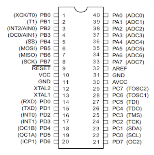
Now about different pins, i will write about ATmega32 because it has more legs.

VCC - power supply (usually 2.7 V - 5.5 V)
GND - ground
RESET - by default we have here log. 1, if we connect it to ground for 2 mcs, MC will be restarted.
XTAL1 - external oscilator input (quartz crystal)
XTAL2 - his output
AVCC - Power supply for ADC converter, it should ALWAYS be connected to VCC
AREF - analog reference pin for the A/D Converter.
ADC(0...7) - ADC input pins, 8 channels,
Port B
(SS, MOSI, MISO, SCK) - are used for data transmission with SPI, also used for programming MC.
(T1, T0) - connects to external clocks, timers T1 and T0 count their impulses..
(AIN0, AIN1) - Analog comparator positive and negative Inputs respectively.
INT2 - External Interrupt pin 2, if we configure it we can get interrupts by changing log. level of tis pin.
OC0 - PW< output
XCK - used with USARTdata transmission
Port C
TDI, TDO, TMS, TCK - used for debugging with JTAG
SDA - Two-wire Serial Bus Data Input/Output Line, DATA, used for data transmission with 2 wires.
SCL - weh we apply impulse here, 1 bit of information is being transmitted from SDA pin.
Port D
ICP1 - (Input Capture PIN) when we have some changes on his pin, we write TIMER1 value in register ICR1.
OC1A - PWM output (register OCR1A)
OC1B - PWM output (register OCR1B)
INT1 - External Interrupt pin 1.
INT0 - External Interrupt pin 0.
TXD - transmit data with USART
RXD - receive data with USART


No comments :
Post a Comment